80+ DRC error: a toolchain issue or a feature?
I want to do some minor modification of the board for testing. Unfortunately, under KiCad 5.0.2, a DRC check of cryptostick.kicad_pcb reports more than 80 errors, including vias clearance issues and items on disabled layers. Should I worry about them? Are these errors here by design, or is it a problem in my toolchain?
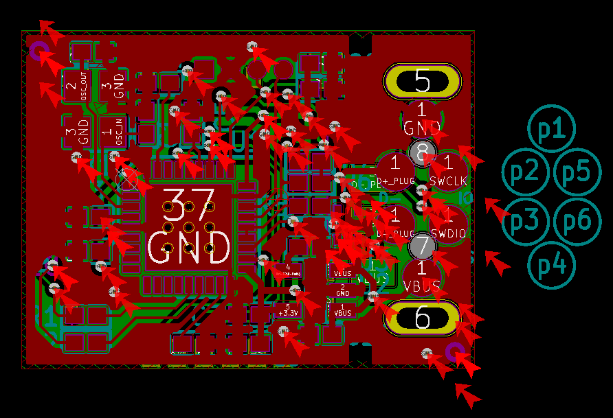
The DRC is not set correctly. Unfortunately KiCad does not always take over the DRC settings correctly. You have to set the minimum track width to 0.15 mm and DuKo to 0.2 mm. Then there should be 8 problems left, all checked and accepted manually.
You have to set the minimum track width to 0.15 mm and DuKo to 0.2 mm.
Sorry, I don't understand the situation. What you've description was in total contradiction with the code. cryptostick.kicad_pcb specifies that,
(setup
(last_trace_width 0.127)
(trace_clearance 0.127)
(zone_clearance 0.15)
(zone_45_only no)
(trace_min 0.127)
(segment_width 0.15)
(edge_width 0.09906)
(via_size 0.5461)
(via_drill 0.381)
(via_min_size 0.5461)
(via_min_drill 0.381)
(uvia_size 0.50038)
(uvia_drill 0.14986)
(uvias_allowed no)
(uvia_min_size 0.50038)
(uvia_min_drill 0.14986)
(pcb_text_width 0.3048)
(pcb_text_size 1 2)
(mod_edge_width 0.09906)
(mod_text_size 0.8 0.9)
(mod_text_width 0.15)
(pad_size 0.3048 0.3048)
(pad_drill 0.3)
(pad_to_mask_clearance 0.05)
(solder_mask_min_width 0.05)
(pad_to_paste_clearance_ratio -0.1)
(aux_axis_origin 127 98.9965)
(grid_origin 119.76 98.05)
(visible_elements 7FFFE67F)
(pcbplotparams
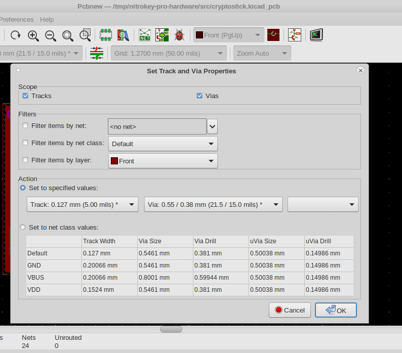
(net_class GND ""
(clearance 0.20066)
(trace_width 0.20066)
(via_dia 0.5461)
(via_drill 0.381)
(uvia_dia 0.50038)
(uvia_drill 0.14986)
(add_net GND)
)
(net_class VBUS ""
(clearance 0.20066)
(trace_width 0.20066)
(via_dia 0.8001)
(via_drill 0.59944)
(uvia_dia 0.50038)
(uvia_drill 0.14986)
)
(net_class VDD ""
(clearance 0.1524)
(trace_width 0.1524)
(via_dia 0.5461)
(via_drill 0.381)
(uvia_dia 0.50038)
(uvia_drill 0.14986)
(add_net +3.3V)
)
In other words,
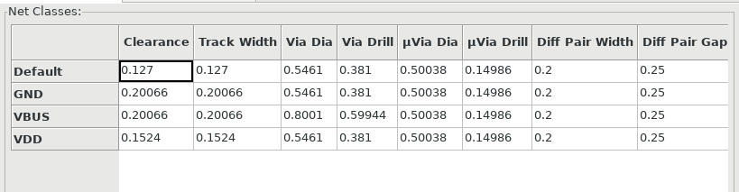
None of the settings match your description. the code says the the minimum track width is 0.127mm for default nets, 0.20mm for Gnd and VBus, and 0.15mm for Vdd.
It also says the minimum vias is 0.5461mm/0.381mm, not 0.2mm. (What is type of vias used in this project, normal vias or microvias? I only see normal vias in the project. not microvias)
Is the layout file or my KiCad somehow broken?
I don't know the internals of cryptostick.kicad_pcb but the settings look different to me.

This is strange.
Are you sure all the changes have been committed to this repository? I was working on git master, commit faa33253b8036cea5b7442066949f93d5b731546, and this is what I see here...
These are default settings which you can set according to your needs. Ideally, change it as suggested above. These settings affect the amount of errors shown to you and affect future changes of the layout.
Agree, it would be nice to have these default settings in the repository correct. We try to fix it in the next revision.
BTW, it looks like you use not the latest version of you layout.
faa3325 is the latest commit in the master branch. Where can I find the latest version of the layout?